
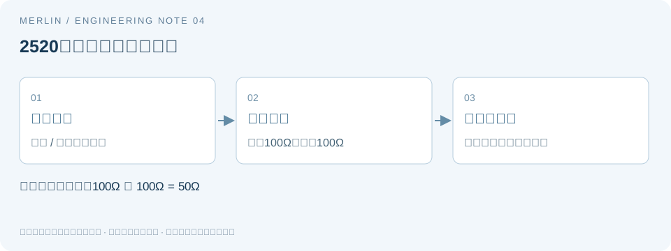
Moving a Differential Oscillator to a 2520 Package
Moving a differential clock to a 2520 package can change the output stage, receiver bias, and trace geometry as well as the footprint. Follow the checks below from the electrical interface through layout. The rise-time example shows why routing may need a fresh review even when frequency stays the same.
1. Check the pinout and electrical interface
2520 describes a nominal package size. Confirm the pin count, supply voltage, and output interface from the datasheet. Orient the old and candidate package drawings the same way and match the power, ground, positive and negative outputs, and control pins one by one. Pay particular attention to top versus bottom views.
Start at the receiver. Record the permissible differential swing, common-mode range, internal bias, and internal termination. Compare these against the oscillator's guaranteed output characteristics. Waveforms on both lines alone cannot establish that the voltage across the pair and the average voltage meet the receiver's requirements.
2. Verify whether internal termination is enabled
An enabled 100 Ω differential termination in parallel with an external 100 Ω resistor yields 50 Ω in a purely resistive model. In a simple current-source model, the termination voltage changes with the load. The actual voltage also depends on the output stage, parasitics, and frequency. Use the datasheet for guaranteed device values.
Verify the receiver's current configuration. Some devices control termination through registers and some offer it only on certain pins or in certain modes. Confirm that the feature is active on the board. Section 2 of TI SNAA377 calls for identifying both driver and receiver conditions.
3. Check edge rates at the same clock frequency
Suppose two candidates both output 125 MHz with an 8 ns period, but their rise times are 1 ns and 0.3 ns. With the same 0.15 ns interconnect propagation delay, the delay-to-rise-time ratios are 0.15 and 0.5, respectively. These ratios illustrate the relative timescales. Acceptable limits depend on the design.
Faster edges contain higher-frequency components, so check discontinuities introduced by traces, vias, pads, and stubs. A long test-point stub can offset the benefit of shorter overall routing. Choose whether to run a transmission-line simulation based on the layer stackup, impedance, length, and device models.
4. Verify static and dynamic behavior on the prototype
Check the supply, enable behavior, decoupling, and output common-mode voltage first. Then measure the differential waveform and valid clock arrival at the receiver, and observe system errors. Where possible, use a suitable differential probe at the receiver. Record the probe load and bandwidth so changes introduced by the measurement can be identified.
For phase jitter comparisons, match the integration band, supply voltage, output frequency, and load. After the prototype passes, archive the exact ordering code and board revision. Specify the tested ordering code in the BOM so that a generic 2520 differential oscillator cannot be substituted without review.
Calculations and Test Records
| Check | Original design | Evidence needed for the candidate |
|---|---|---|
| Package and pins | Original board footprint drawing | Pads, pin assignments, and height in a common orientation |
| Receiver termination | External, internal, or disabled | Verify the mode in use |
| Output characteristics | Frequency and interface | Common mode, swing, edge rates, and enable behavior |
| System validation | Original board as a control | Same supply, temperature range, and measurement method |
References and Scope
This analysis draws on public sources and was prepared with AI assistance. All examples use hypothetical values. Confirm product specifications and compatibility against the exact ordering configuration, the latest manufacturer datasheet, and board-level validation.
Manufacturer reference Texas Instruments SNAA377, December 2025, Differential and Single-Ended Signal Termination Guide, Sections 2–4.
Related Selection Guides
For BOM and RFQ fields, see MERLIN's guide to differential oscillator interfaces, packages, and selection. Confirm device specifications against the applicable manufacturer datasheet and project validation.