
Does 0.1 mm in a CSP Clock Datasheet Refer to Stencil Thickness or Device Height?
Question and manufacturer guidance
For compact clock devices, package dimensions, recommended land patterns, and stencil notes often appear next to one another. Keep each dimension with its original label so package and assembly reviews use the correct value.
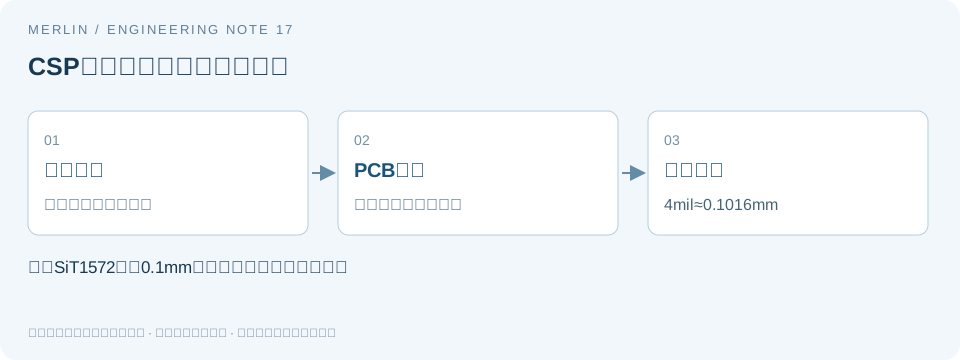
On page 5 of the SiTime SiT1572 Rev 2.0 datasheet, a note next to the recommended land pattern recommends a 4 mil (0.1 mm) stencil. Record this under stencil thickness. Device body height, pad spacing, and post-reflow standoff have separate dimensions.
Engineering analysis and limits
Organize dimensions by physical item. Body height belongs to the component, pad dimensions to the PCB, and stencil thickness and apertures to the solder paste printing tool. They share a unit. Retain the original field names before converting units so a note from a neighboring drawing stays with the right item.
The exact conversion is 4 mil = 0.004 in × 25.4 = 0.1016 mm. The datasheet rounds this to 0.1 mm. The conversion applies to the stencil recommendation. Check device height and post-reflow standoff using their own data.
For a simple geometric estimate, assume a 0.20 mm² aperture area and a 0.10 mm stencil thickness. The theoretical aperture volume is 0.020 mm³. At 0.12 mm it is 0.024 mm³, an increase of 20%. This corresponds to area times thickness. Actual paste transfer and solder joint volume require process verification.
Verification steps
Keep the component drawing, recommended land pattern, solder mask openings, stencil apertures, and stencil thickness as separate records. Obtain any post-reflow standoff and actual paste transfer efficiency that the manufacturer does not specify from project documentation or process validation.
When changing parts on an existing PCB, compare the existing land pattern with the candidate's recommendation before deciding whether to reuse the stencil. Record the equipment, solder paste, placement, and reflow conditions. Limit the result to the specific process revision and check the full assembly process for equivalence.
Check and record table
| Item or condition | Check or calculation | Interpretation and limits |
|---|---|---|
| Exact conversion of 4 mil | 0.1016mm | The datasheet rounds to 0.1 mm |
| Dimension recorded | Stencil thickness | Device height is a separate field |
| Hypothetical 0.20 mm² × 0.10 mm | 0.020mm³ | Theoretical geometric volume |
| Increase thickness to 0.12 mm | Theoretical volume increases by 20% | Verify actual transfer separately |
Manufacturer documentation and applicability
https://www.sitime.com/datasheet/SiT1572
AI assisted in preparing this article. The manufacturer requirements and the engineering analysis are presented separately. Unless explicitly identified as manufacturer specifications, all worked examples are hypothetical and were not verified on samples. Use the specific datasheet and project validation to determine specifications and compatibility for a candidate part.
Related selection guides
For help documenting these parameters in a BOM or RFQ, see MERLIN’s active oscillator package and selection documentation. Confirm specific part parameters against the applicable manufacturer datasheet and project validation.