
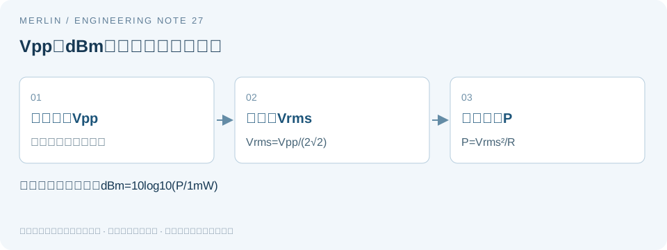
Convert a sine wave measured across the load
For an ideal sine wave with zero DC offset measured across resistance R, Vrms = Vpp/(2√2) and P = Vrms²/R = Vpp²/(8R). Convert power in watts using dBm = 10 log₁₀(P/0.001 W).
At 1 Vpp across 50 Ω, Vrms ≈ 0.353553 V, P = 2.5 mW and the result is approximately 3.9794 dBm. Using Vpp as Vrms instead would overstate calculated power by a factor of eight.
| Sine wave across 50 Ω | Power | dBm |
|---|---|---|
| 0.5 Vpp | 0.625 mW | −2.0412 |
| 1.0 Vpp | 2.5 mW | 3.9794 |
| 2.0 Vpp | 10 mW | 10.0000 |
Why a high-impedance reading can be larger
An ideal source with 50 Ω series resistance and 2 Vpp open-circuit output delivers 1 Vpp to a matched 50 Ω load. A very high-impedance input reads close to 2 Vpp. Treating that 2 Vpp as a measurement across 50 Ω would imply 10 mW in place of 2.5 mW, an error of four times, or 6.0206 dB. This result depends on the assumed impedances and operating frequency.
CMOS clocks require their specified load
For a square wave with DC offset, total RMS, AC RMS and fundamental RMS differ. A spectrum analyzer reading at one frequency depends on harmonics, bandwidth and settings. A sine-wave formula does not convert arbitrary CMOS clock Vpp.
For example, section 1 of the Taitien NF-10M-7000 Series datasheet specifies a CMOS output. Section 1.7 specifies 10 kΩ in parallel with 15 pF. A direct 50 Ω termination changes the test condition.
Acceptance records
Record ordering code, waveform, specified load, probe or attenuator, instrument impedance, coupling and test point. Document any buffer or matching network and calibration. At high frequencies, probe capacitance and routing affect the load even when an instrument is labeled high impedance.
References and scope
MERLIN used AI assistance to compile this technical guide. Numerical examples are hypothetical unless identified as manufacturer specifications. They are not sample measurements, compatibility guarantees, or statements of availability.