
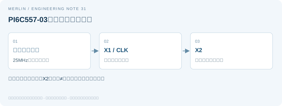
How to handle X2 when driving the PI6C557-03 with a single-ended 25 MHz clock
Manufacturer requirements
A clock generator can support both a crystal reference and an external single-ended clock, with different connections for each. Record the selected reference input configuration when documenting a part change.
The pin table in PI6C557-03 datasheet DS43154 Rev2-2 specifies that X1/CLK accepts a 25 MHz crystal or single-ended clock. When using a clock input, leave X2 unconnected to ground and all other nets.
Circuit changes when switching reference inputs
Draw the crystal and external oscillator options as separate configurations. In the crystal configuration, the crystal and its associated circuit connect to X1/CLK and X2. In the external clock configuration, the clock drives X1/CLK and X2 stays open, as specified in the pin table.
When changing from a crystal to an external oscillator, review the existing crystal, the surrounding components on both sides, PCB nets, and any test points. Update the schematic and BOM together. Use the full manufacturer input requirements to determine which external components to remove or change.
The pin table defines the pin functions. Check allowable clock amplitude and loading separately, along with driver output levels, receiver input conditions, control pins, and power-up behavior.
Verification steps
Use the netlist to check where X1/CLK connects, whether X2 still has an external connection, and how the associated capacitors and test points are handled. Cross-check schematic pin numbers, PCB pads, and the datasheet's top or bottom view using the documented pinout.
On the prototype, confirm the reference source and input mode, then check the waveform at the receiver and verify the output function. Record the full device revision and input configuration. Check the unused-pin requirements for each clock generator model separately.
Verification checklist
| Item or condition | Check or calculated result | Notes and limits |
|---|---|---|
| Crystal reference configuration | Follow the manufacturer's crystal circuit | Document separately from the external clock configuration |
| External clock configuration | Clock drives X1/CLK | Verify electrical requirements separately |
| X2 with an external clock input | Leave unconnected | Leave it electrically unconnected |
| Verification records | Netlist, mode, waveform, and device revision | Verify connectivity against the netlist and schematic |
Manufacturer documentation and scope
https://www.diodes.com/datasheet/download/PI6C557-03.pdf
MERLIN used AI to help prepare this guide. The manufacturer documentation specifies device requirements, and the worked examples use hypothetical values. Confirm device specifications and compatibility with the applicable datasheet and sample testing.
Related selection guides
For BOM and RFQ preparation, see MERLIN guide to verifying Diodes / Pericom clock part numbers and documentation. Verify the specific part using its manufacturer datasheet and project testing.