
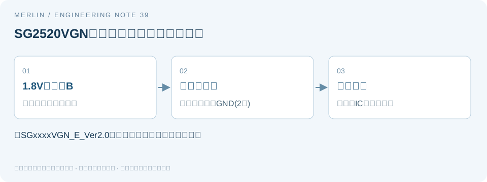
Can the 1.8 V SG2520VGN use output option B?
Manufacturer requirements
When sourcing a configurable differential oscillator, verify the exact supply and output combination. The manufacturer may list both options individually while excluding their use together.
Pages 2 and 3 of Epson's full SG2016VGN and SG2520VGN datasheet, SGxxxxVGN_E_Ver2.0, state that output option B is unavailable with the 1.8 V typical supply. When selecting the low-voltage version, verify the entire ordering code, including the output option.
Verifying orderable combinations
Check a matrix of allowed configurations. A supply voltage listed for the series and an output option listed in the electrical table may be mutually exclusive in a single ordering code. Check footnotes when screening options.
Put supply voltages in rows and output options in columns. Mark each combination as allowed, excluded, or pending verification. The documentation rules out 1.8 V with option B. Verify the other combinations from the full datasheet, including other output options at 1.8 V.
If you change the output option to keep the supply voltage, review receiver swing, common mode, current, and termination. The output option letter can specify electrical differences that require a circuit review before the BOM changes.
Verification steps
Before ordering samples or production quantities, enter the supplier-confirmed full ordering code in the matrix and include the manufacturer document revision and applicable entry. Keep the product family page, configuration matrix, and confirmed ordering code in the record so you can compare the quoted configuration with the request.
Use the datasheet to verify a configuration and the supplier's order confirmation to verify availability. Leave unconfirmed part numbers, stock, and lead times marked as pending.
Verification checklist
| Item or condition | Check or calculated result | Notes and limits |
|---|---|---|
| Product family | 1.8 V supply option available | Check which outputs are allowed at this voltage |
| Supply and output combination | Manufacturer excludes 1.8 V with option B | Verify both options together |
| Output option change | Recheck receiver conditions | Review the circuit before changing the ordering code |
| Complete ordering code | Manufacturer document revision and confirmed configuration | Match samples to the BOM |
Manufacturer documentation and scope
https://download.epsondevice.com/td/pdf/app/SG2520VGN_en.pdf
MERLIN used AI to help prepare this guide. Manufacturer documents specify device requirements. The engineering examples are hypothetical. Confirm device specifications and compatibility with the applicable datasheet and sample testing.
Related selection guides
For BOM and RFQ preparation, see MERLIN guide to differential oscillator supplies, outputs, and part selection. Verify the specific part using its manufacturer datasheet and project testing.
Why the SG2520VGN side terminals must remain isolated
Two differential oscillators in 2520 packages can look similar while their exposed metal features are connected differently. Review the top cover and side terminals against nearby conductors as well as checking the bottom pads.
Two separate manufacturer precautions
In the usage precautions for the Epson SG2016VGN and SG2520VGN, datasheet SGxxxxVGN_E_Ver2.0, item 8 states that the top metal cover connects directly to the GND terminal at pin 2. Item 21 states that the side terminals connect internally to the IC and must be protected against shorts and reduced insulation resistance. The precautions apply to different metal features.
Use the specified GND connection for testing and check side clearances against documentation for the actual device and assembly. These two precautions describe the SGxxxxVGN devices covered by the datasheet. Verify other series using their own documentation.
Document the physical location of each metal feature
Include top, bottom, and side views of the candidate part in one record. Label the designated GND pad, top cover, and side terminals. Mark any exposed metal whose function the manufacturer leaves undefined as pending verification. A single continuity reading establishes only the connection measured. Keep unknown terminals isolated during verification.
Record the physical location, documented electrical function, nearby board conductors, and corresponding assembly risks. Keep non-ground conductors clear of the grounded top cover. Protect side terminals against shorts and reduced insulation resistance as directed by the manufacturer.
Assembly checks beyond the CAD footprint
The footprint defines the designed connections. Solder, rework, nearby components, and shielding can change the as-built clearances. Review the existing PCB, candidate part, and assembly revision together when evaluating the 2.5 × 2.0 mm replacement.
For example, if you add a ground spring beside the oscillator, identify precisely where it could make contact. Check that point against both the device and mechanical design documents before approving the spring arrangement.
Verification records
Record the complete ordering code, datasheet revision, and package orientation, and keep photos before and after assembly. Inspect appearance and connections with power off according to the project procedure. Run powered tests separately at the specified supply, termination, and load. If an anomaly appears, record the point of contact and the circuit node along with the oscillator symptom.
A passing sample covers its tested clearances, solder volume, and mechanical condition. Set production acceptance criteria from the device documentation, PCB design, and assembly verification.
Manufacturer documentation · Epson SGxxxxVGN_E_Ver2.0, usage precautions 8 and 21. For related interface checks, see MERLIN differential oscillator specification checklist。
MERLIN used AI to help prepare this analysis of public documentation and suggested checks. Verify board performance, stock, and compatibility separately.