
Start with the receiver
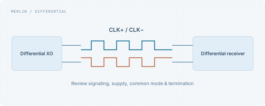
Read the FPGA, PHY or other receiver clock-input specification, including supported signaling, input swing, common-mode conditions and reference circuits. Differential interfaces are not automatically interchangeable.
Frequency, voltage and package are not enough
Also review output pin assignments, OE/NC definitions, coupling and termination. Use guidance for the selected driver and receiver rather than treating one product family reference circuit as universal.
Compare jitter with its conditions
Read RMS phase jitter with its integration band. Values taken under different bands or conditions should not be directly compared; supply, routing and measurement methods affect system results.
A complete differential-clock inquiry
Include frequency, signaling type, supply, package and pin count, temperature range, jitter and integration band, receiver, quantity and target delivery. Preserve the complete ordering code when replacing an existing part.