
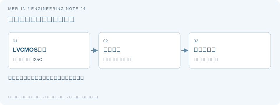
Why a circuit driving a differential input from LVCMOS assumes a 25 Ω source
Manufacturer requirements
When using an application diagram that connects a single-ended clock to a differential receiver, document the assumptions behind the resistor values. If the clock source changes, check whether the same external components still apply.
Section 9 of SiTime AN10029 states that the component values in Figures 23 and 24 assume a 25 Ω LVCMOS driver impedance. This is typical for the SiT8008 series. When using the example for another LVCMOS oscillator, check that device's impedance.
Sensitivity to source impedance
Treat the driver impedance as part of the circuit. LVCMOS drivers can have different effective output impedances depending on the series, supply voltage, and drive setting. Use the manufacturer's typical 25 Ω value under its documented conditions. Verify guaranteed minimum and maximum values separately if the design requires them across temperature.
A simple resistor model illustrates the effect. For an equivalent source voltage Vs in series with source resistance Rs and a 50 Ω resistive load, load voltage is Vs × 50 / (Rs + 50). The ratio is approximately 0.667 at Rs = 25 Ω and 0.5 at Rs = 50 Ω. Only the source resistance changed. The hypothetical 50 Ω load illustrates sensitivity to source impedance. Determine actual loading from the circuit and oscillator specifications.
The real differential receiver network also includes coupling, resistor division, internal bias, and frequency response. Use the DC model to understand why the source impedance assumption matters, and analyze the full circuit to choose termination values.
Verification steps
Set up two columns for the application diagram and the current project. Compare the source part number, supply, drive setting, load, receiver, coupling, and termination. Flag unknowns and resolve them with device documentation or testing. Determine output impedance directly from these sources.
Observe the waveform at the receiver input, and record the probe and network conditions. An unloaded waveform or a square wave observed only at the source leaves the receiver's swing, common mode, and timing requirements unverified.
Verification checklist
| Item or condition | Check or calculated result | Notes and limits |
|---|---|---|
| Application diagram assumption | SiT8008 typical impedance of 25 Ω | Check guarantees for the actual LVCMOS source |
| Simplified model with Rs = 25 Ω and RL = 50 Ω | VL/Vs≈0.667 | Hypothetical sensitivity calculation |
| Simplified model with Rs = 50 Ω and RL = 50 Ω | VL/Vs=0.5 | Illustrative load for the simplified model |
| Current project | Document driver, receiver, bias, and load separately | Confirm compatibility after verifying circuit conditions |
Manufacturer documentation and scope
https://www.sitime.com/output-terminations-differential-oscillators
MERLIN used AI to help prepare this guide. The manufacturer documentation specifies device requirements, and the worked examples use hypothetical values. Confirm device specifications and compatibility with the applicable datasheet and sample testing.
Related selection guides
For BOM and RFQ preparation, see MERLIN guide to differential clock interfaces and termination. Verify the specific part using its manufacturer datasheet and project testing.