
Checking common mode and termination for 125 MHz AC- and DC-coupled clocks
A 125 MHz clock has a defined period. To read it reliably, the differential receiver needs adequate swing and a valid input common-mode voltage. The following hypothetical voltages show how to check both and why AC coupling still requires bias.
1. Calculate differential and common-mode voltage
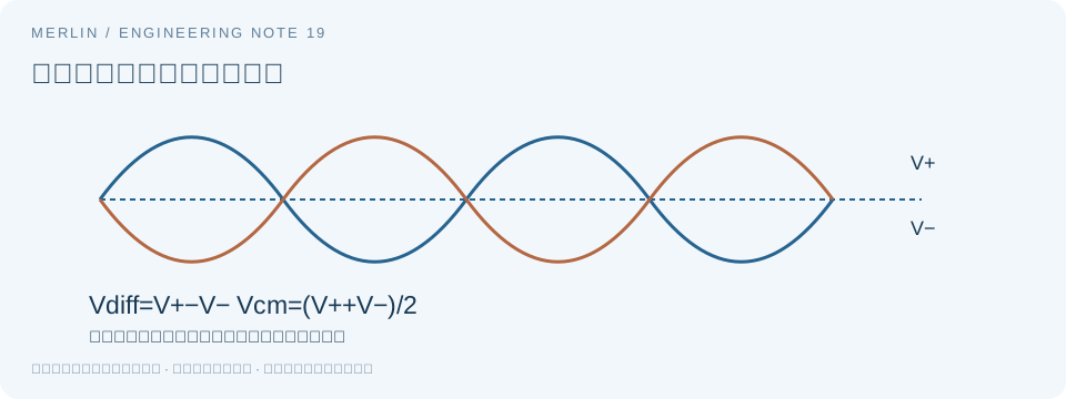
Define Vdiff = VP − VN and Vcm = (VP + VN) / 2. When P = 1.4 V and N = 1.0 V, Vdiff = +0.4 V and Vcm = 1.2 V. When the signal reverses, P = 1.0 V and N = 1.4 V. Vdiff is then −0.4 V, common mode remains 1.2 V, and the differential peak-to-peak voltage is 0.8 V.
The voltages are hypothetical. When reviewing an LVDS or other 125 MHz device, distinguish single-ended swing from differential peak-to-peak swing and account for each value's measurement conditions.
2. Check both endpoints for DC coupling
DC coupling passes DC levels from the driver to the receiver. Compare the guaranteed output common-mode range with the receiver's allowed range, and check differential swing, absolute maximum ratings for each pin, power sequencing, and powered-down states. Check the entire range even when the typical value is within the receiver's limits.
Suppose the receiver accepts 1.0–1.4 V common mode and the candidate driver guarantees 0.9–1.3 V. The ranges overlap, but the driver's 0.9–1.0 V portion below the receiver minimum falls outside the receiver's allowed range. Verify that the receiver covers the full guaranteed output range.
3. Set the receiver bias for AC coupling
With series coupling capacitors, internal self-bias or an external network must set the receiver's common-mode voltage. Confirm that the input supports AC coupling and check how it is biased. Use the network recommended for the specific receiver.
The coupling capacitance and effective impedance form a high-pass response. Choose capacitance based on signal frequency, allowable amplitude variation, and startup and stop behavior. A continuous 125 MHz clock, a low-frequency pulse, and a single SYSREF event impose different conditions. Verify output stage and receiver compatibility even when increasing coupling capacitance.
4. Verify termination and jitter independently
Choose termination based on the output type and receiver structure. LVDS, LVPECL, HCSL, and low-power HCSL use different output stages and can require different networks. Check termination placement, PCB impedance, and possible duplication of internal resistors.
Measure the waveform at the receiver and check system operation. Phase jitter, period jitter, and cycle-to-cycle jitter are distinct measurements. Follow the receiver's requirements and record measurement bandwidth and integration range. Accept the design only after checking termination, jitter, and common-mode compliance individually.
Calculation and recording table
| Example condition | Result | Purpose |
|---|---|---|
| P=1.4V、N=1.0V | Vdiff=0.4V;Vcm=1.2V | Distinguish differential and common-mode voltage |
| Swap P and N | Vdiff=−0.4V | Differential peak-to-peak swing is 0.8 V |
| Output 0.9–1.3 V, input 1.0–1.4 V | Part of the output range falls outside the input range | Compare the full guaranteed ranges |
| After AC coupling | The receiver needs its own common-mode bias | Check internal or external bias |
References and scope
MERLIN used AI to help prepare this analysis of public documentation. All example conditions are hypothetical. For a specific part, use the exact ordering configuration, the current manufacturer datasheet, and whole-board verification to confirm specifications and compatibility.
Manufacturer reference · Texas Instruments SNAA377, Differential and Single-Ended Signal Termination Guide, December 2025, Sections 2–4。
Further reading
MERLIN guide to differential oscillator interfaces and termination covers checks for output logic, receiver bias, and termination. Use the TI application note and device datasheets as the primary references.