
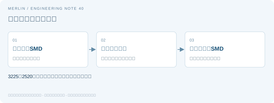
Two-Pad and Four-Pad Footprints for 3225 Crystals
Manufacturer Drawings
3225 identifies nominal body dimensions. Check the recommended footprint for the exact series against the existing PCB copper to decide whether replacement requires a board change.
KDS publishes a combined catalog for DSX321G, DSX321GK, and DSX320GE. The recommended footprint has four pads for DSX321G and DSX321GK and two larger pads for DSX320GE. All three are in the 3.2 × 2.5 mm size class, and their different land patterns matter to the design.
Comparing the Land Patterns
Check the package outline and recommended land pattern separately. The 3.2 × 2.5 mm outline describes the component envelope. Pad length, spacing, and count come from the separate land-pattern drawing. Build the PCB library footprint from the exact series drawing because the 3225 designation gives nominal body size only.
For four-pad packages, identify the crystal terminals and any pads connected to the case or designated for ground. For two-pad packages, verify the specified pad positions. Use documented pin assignments and check mechanical soldering compatibility even when both devices have two electrical terminals.
Overlay the drawings in a common orientation and record the top or bottom view, coordinate origin, and units. Check copper overlap, solder-mask openings, component rotation, and surrounding clearance. Aligning the package centers alone cannot establish a match.
Board and Assembly Validation
Save the original footprint, the manufacturer's candidate drawing, and a list of differences from the overlay. Have the hardware and manufacturing teams determine whether the PCB revision must change. Confirm soldering, mechanical retention, and electrical continuity as well as initial pad contact.
If the existing PCB supports a compatible land pattern, record the copper layout and assembly validation. Otherwise, document the board change. The catalog comparison illustrates how to identify different footprints. Assess other two-pad and four-pad devices against the specific board and process.
Inspection Record
| Item or condition | What to verify | Acceptance basis |
|---|---|---|
| Device outline | Length, width, and height drawing | Check the land pattern separately |
| Land pattern | Two or four pads | Use the drawing for the exact series |
| View and coordinates | Top or bottom view, orientation, and units | Normalize before overlaying |
| Final disposition | Specific PCB and assembly revisions | Use drawings and validation to confirm the specific 3225 footprint |
Manufacturer Reference and Scope
https://ftp.kds.info/products/DSX321G_GK_320GE_car_en.pdf
This guide was prepared with AI assistance. Manufacturer specifications and engineering conclusions are identified separately. Worked examples are hypothetical unless identified as manufacturer data and were prepared without sample measurements. Validate specifications and compatibility for the exact part through documentation and testing.
Related Selection Guides
For BOM and RFQ fields, see MERLIN's guide to passive crystal packages and part numbers. Confirm specifications against the applicable manufacturer datasheet and project validation.