Crystal Oscillator

Home    >   Commitment   >   Application Notes   >   Crystal Oscillator
Crystal Oscillator - Technical terms
Crystal Oscillator - Application notes
Crystal Oscillator - Reliability specifications


◆ Technical Term ◆

Nominal frequency:
The enter or nominal output frequency of a crystal oscillator.

Package:
Crystal oscillators are packaged in various styles from lead through holes to surface-mount types. Various sizes and functions are suitable for different applications.

Frequency tolerance:
The deviation from the nominal frequency in terms of parts per millions (ppm) at room temperature.(25°C±5°C)

Frequency range:
The frequency band that the oscillator type or model can be offered.

Frequency stability:
The maximum allowable frequency deviation compared to the measured frequency at 25°C over the temperature window, i. e., 0°C to +70°C typical stability is 0.01% (100 ppm).

Operable temperature:
Temperature rang within which output frequency and other electrical, environmental characteristics meet the specifications.

Aging:
The relative frequency change over a certain period of time. This rate of change of frequency is normally exponential in character. Typically, aging is ±5ppm over 1 year maximum.

Storage Temperature:
The temperature range where the unit is safely stored without damaging or changing the performance of the unit.

Frequency vs. Power Supply Variation:
Maximum frequency change allowed when the power supply voltage is changed within its specified limits (typical 10% in Vcc or ±5% change).

Supply Voltage (Vdd max):
The maximum voltage which can safely be applied to the Vcc terminal with respect to found. Maximum supply voltage for TTL and CMOS is 5.5V

Input Voltage (VIN):
The maximum voltage that can be safely applied to any input terminal of the oscillator.

Output Voltage (VOH):
The minimum voltage at an output of the oscillator under proper loading.

Input HIGH Voltage (VIH):
The maximum voltage to guarantee the threshold trigger at the input of the oscillator.

Input HIGH Voltage (VIL):
The minimum voltage to guarantee the threshold trigger at the input of the oscillator.

Supply Current (Icc):
The current flow into Vcc terminal with respect to ground. Typical supply current is measured without load.

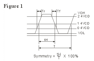
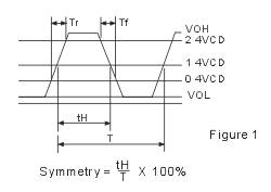
Symmetry or Duty Cycle:
The symmetry of the output waveform at the specified level (at 1.4V for TTL, at 1/2 Vcc for CMOS, or 1/2 waveform peak level for ECL)


Fan Out:
The measure of driving ability of an oscillator, expressed as the number of inputs that can be driven by a single output. It can be represented by an equivalent load capacitance (CL) or a TTL load circuit consisting of diodes, load resistor, and a capacitor.

Rise Time (Tr):
Waveform rise time from Low to High transition, measured at the specified level

10% to 90% for CMOS,
20% to 80% for ECL
0.4V to 2.4V for TTL.

Fall Time (Tf):
The waveform fall time from High to Low transition, measured at the specified level

90% to 10% for CMOS,
80% to 20% for ECL
2.4V to 0.4V for TTL.
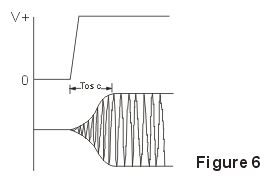
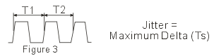
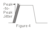
Jitter:
The modulation in phase or frequency of oscillator output.
CMOS/TTL Compatible: The oscillator is designed with CMOS logic with driving capability of TTL and CMOS loads while maintaining minimum logic HIGH of the CMOS.

Tri-state Enable:
When the input is left "open" or tied to logic "1", the normal oscillation occurs. When the input is grounded (tied to logic "0"), the output is in "high impedance" state. The input has an internal pull-up resistor thus allowing the input to be left open.

Output Logic:
The non-linear distortion due to unwanted harmonic spectrum component related with target signal frequency. Each harmonic component is the ratio of electric power against desired signal output electric power and is expressed in terms of dBc, i.e.-20dBc. Harmonic distortion specification is important especially in sine output when a clean and less distorted signal is required.
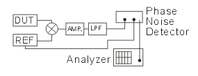
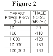
Phase Noise:
The measure of the short-term frequency fluctuations of the oscillator. It is usually specified as the single side band (SSB) power density in a 1 Hz bandwidth at a specified offset frequency from the carrier. It is measured in dBc/Hz.

Stand By:
A function that temporary turns off the oscillator and other devices to save power. Logic "0" will enable stand by mode. The disable current at stand by mode varies from a few micro-amperes to tens of micro-amperes (5 A typical). Because oscillation is halted, there is a maximum of 10 ms (same amount of start-up time) before output stabilizes.


Back to top
◆ Application Notes ◆

CMOS Rise and Fall Times

The rise and fall time on the CMOS technology depends on its speed, the supply voltage, the load capacitance, and the load configuration.
Typical rise and fall time for CMOS FN series is 10ns.
Typical rise and fall time is measured between 10% to 90% of its waveform level. (See example of Wave Output; Fig. 1.)


CMOS Output Termination Techniques
Due to the fast transition time of the CMOS (TTL compatible)device, proper termination techniques must be used when testing or measuring electrical performance characteristics. Termination is usually used to solve the problem of voltage reflection, which essential cause steps in clock waveforms as well as overshoot and undershoot. Such effect could result in false clocking of data, as well as higher EMI and system noise.

Termination is required also because of the length of the trace on the PC board and its load configuration.

There are three general methods of terminating a clock trace. Which is a process of matching the output impedance of the device with the line impedance:

1) Series termination
2) Pull-up / Pull-down termination
3) Parallel-AC termination

METHOD 1:

In series termination, a damping resistor is placed close to the source of the clock signal. Value of Rs must satisfy the following requirement:


METHOD 2:


In pull-up / pull-down termination, the Thevenin=s equivalent of the combination is equal to the characteristics impedance of the trace.
This is probably the cleanest, and results in no reflections. As well as EMI.


METHOD 3:


In parallel AC termination, a R-C combination is placed at the load. The value of the capacitor must be chosen carefully, usually smaller than the 50pF. This termination is not recommended because it will degrade the rise and fall time of the clock, although it draws no DC current.


Overall Frequency Stability:
The crystal oscillator is typically used as a master clock for the microprocessor and its parameters are not affected by the internal characteristics of the microprocessor such as variation in load capacitance and other variables that could affect the change in frequency at room and over temperature. The overall frequency stability in crystal oscillators is typically ±100ppm max. And includes frequency calibration at 25°C over temperature, frequency changes due to load, supply, aging, vibration, and shock.


Start-up Time:
Start-up time is the delay time between the oscillation starts from noise until it reaches its full output amplitude when power is applied. The supply voltage must be applied with a defined rate or rise. The start-up time varies from microseconds to milliseconds depending on frequency, ASIC speed and logic, Please see figure 6

Figure 6

Tri-state Enable / Disable Mode
When the voltage at the control pin is set to at logic low "0" output is in Tri-state mode that is High impedance. The disabled current is usually lower than its normal operation current but not completely cut-off as it was seen in the Stand-by mode, where the oscillation is shut down completely.
There is an internal pull-up resistor between control pin and supply pin (typically 100k ohms), Therefore the control pin can be left open (floating) if unused.


Phase Noise and Measurement
Phase noise is the expression of noise in the frequency domain. It is a measure of the short-term frequency fluctuations of the oscillator. It is usually specified as the single sideband power density in a 1 Hz bandwidth at a specified offset frequency from the carrier.


In order to measure phase noise, it is necessary to pair a similar device-
under-test with one unit set a VCXO and other set


a fixed XO. Please see block diagram in figure 2. Typical phase noise in VCXO and oscillators:


Jitters and Its Types
Jitter is noise caused by many sources in crystal oscillators.
Major sources of noise are:

  • Power supply noise.
  • Integer multiples of the signal source frequency (harmonics).
  • Load and termination conditions.
  • Amplifier noise.
  • Circuit configuration (PLLs, Multiplier, Overtone, etc.)
The following methods can be used to suppress the noise conditions in the above sources:
  • Make sure that the power supply noise is filtered by using bypass capacitors, chip beads, or RC filters.
  • If jitter is critical in some applications, especially for high-frequencies noise, use low harmonics outputs or sine-output.
  • Make sure that load and termination conditions are optimized to avoid reflected power back to its output.
  • Typically, PLLs, Multiplier or Programmable designs produce higher jitter than the conventional fundamental design. It is very important to understand the jitter requirements from the application to specify the right specification for crystal oscillators.

We can classify two types of jitters:

  • Cycle to cycle jitter
  • Period jitter
Cycle to Cycle Jitter
The Cycle to cycle jitter is the maximum difference in time between several measured periods. Usually a minimum of ten(10) cycles is used where T1 to T10 were recorded. See Fig. 3

Period Jitter
The period jitter is the maximum change of a clock edge. It is usually expressed as peak-to-peak jitter and can be converted to rms value by multiplying to (0.5)x(0.707). The period jitter can only be measured at each cycle but not multiple cycles. See figure. 4
Typical jitter recorded in oscillators varies from 20ps to 60ps rms.


Electrical Handling and Layout
1) By pass Capacitor

Although many metal can oscillators have built-in bypass capacitors for SMD crystal oscillators. It is a good practice to add an external bypass capacitor 0.01μ F near the Vdd terminal. The external capacitor is used as an over impressed voltage and overcorrect protective device.


Figure 1
shows a typical layout for a surface-mount crystal oscillator.

2) Load Impedance
Oscilloscope impedance shall be greater than 1 M ohms with probe capacitance less than 15pF, The load applied shall include probe capacitance. All lead length should be kept as short as possible especially ground trace. Output trace from oscillator output to the load (next IC) shall be kept short and avoided layout in parallel or cross with another hot signal trace. Stray capacitance and inductance have major effects on output impedance of the oscillator unit and shall be minimized.

3) Output frequency
Output frequency shall be measured with a precision frequency counter using a reference external tine base. Make sure to stabilize the crystal oscillator (warm-up) before recording the final frequency value, especially on high frequency and high current units.


Mechanical
1) Vibration and shock
Do not apply or cause sudden shock and vibration exceeding its maximum specifications to the unit. Severe drop or hit with a hard object could damage the unit electrically and mechanically. Please check the unit if dropped before assembling or using.

2) Mounting
The following precautions shall be applied to all surface mount oscillators:
Use the appropriate reflow condition as recommended on the unit specification. Please make sure to not exceed the peak temperature, its maximum duration, the number of exposures, the rate of temperature change vs. Time, etc.

Do not apply excessive soldering heat or soldering duration on terminals.

Packaging
Although an anti-static protection circuit is built-in the ASIC. Excessive static electricity level may damage the unit. PSE Technology uses conductive packing materials for some oscillators be sure to ground with ESD strap before handling the device.

Handing Unused Terminals
Some PSE Technology oscillators include Tri-state function. Although there is an internal pull-up resistor to prevent floating, it is recommended to terminate the tri-state terminal to Vdd with a resistor of 100k ohms in series.

Storing
Please store all units at normal temperature and humidity. High humidity may cause deterioration to units. Avoid storing over a long period. Please perform visual and electrical inspections before using once the units are stored over a long period.


Back to top
◆ Reliability Specification ◆

MECHANICAL CHARACTERISTICS


VIBRATION

20G, 10~2000Hz sweep for 20 minutes, 1.52mm, 4 hours for each direction.
Ref. MIL-STD-883E Method 2007.2

MECHANICAL SHOCK
100G, 0.5mS, 3 times for each direction
Ref. MIL-STD-883E Method 2002.3

DROP TEST
75cm Height, 3 times on 2mm stainless plate.
Ref.JIS C6701

SOLDERABILITY
95% coverage by using 63/37 solder at 230±5°C solder pot immersion 3 ± 0.5 seconds.
Ref.MIL-STD-883E Method 2003.7

RESISTANCE TO SOLDER HEAT
10 seconds±5 seconds immersion into 260±5°C solder pot. Ramp rate is 1 to 4°C/sec; above 183°C is 90~120 seconds.
Ref. MIL-STD-202 Method 210, test condition J.

GROSS LEAK TEST
5kgf/cm2 Helium bombing for 2 hours, bubble test in 125±5°C FC # 40 for 60 Second or equivalent auto test method.
Ref. MIL-STD-883E Method 1014.10

FINE LEAK TEST
5kgf/cm2 Helium bombing for 2 hours, leak rate less than 1X10 exp (-8)atm.c.c./sec.
Ref.MIL-STD-883E Method 1014.10

DIMENSION CHECK
X,Y,Z three dimensional, according to specifications
Ref. MIL-STD-883E Method 2016

DPA (INTERIOR CHECK)
Visual and 50X Stereo-microscope.
Ref. MIL-STD-883E Method 2013.1


ENVIROMENRAL CHARACTERISTICS


THERMAL SHOCK
-55°C~125°C for 100 cycles, dwell time: 30 minutes,
Transit time less than 10 minutes
Ref. MIL-STD-883E Method 1011.9

HIGH TEMPERATURE STORAGE
125±3°C 1000±12hours.
Ref. MIL-STD-883E Method 1055.4

LOW TEMPERATURE STORAGE
-55±3°C static 1000±12hours.
Ref. MIL-STD-833E Method 1013

HIGH TEMP. AND HIGH HUM. DITY
-40±3°C RH 85%, 1000 hours.
Ref. MIL-STD-833E Method 1004.7

FREQ. Vs. TEMPERATURE
-40°C~85°C , from low temp. 5°C step up to high temp


Back to top


Copyright © Shenzhen Merlin Electronics Co.,Ltd. 2010
Room 801A, Huiheng Building Phase 2, Hi- tech South 7th Rd., Hi-tech Park, Nanshan Dist., Shenzhen,China
Phone:86-755-26500570 Fax:86-755-26068952 E-mail: sales@mecxtal.com.cn