|
Seam Sealed Ceramic Surface Mount Crystal Package
 MECHANICAL CHARACTERISTICS MECHANICAL CHARACTERISTICS
 VIBRATION VIBRATION
20G, 10~2000Hz sweep for 20 minutes, 1.52mm, 4 hours for each direction.
Ref. MIL-STD-883E Method 2007.2
MECHANICAL SHOCK
1000G, 0.5mS, 3 times for each direction
Ref. MIL-STD-883E Method 2002.3
DROP TEST
75cm Height.3 times on 2mm stainless plate.
Ref.JIS C6701
SOLDERABILITY
95% Coverage by using 63/37 solder at 230±5°C solder pot immersion 3±0.5 seconds.
Ref.MIL-STD-883E Method 2003.7
RESISTANCE TO SOLDER HEAT
10 Seconds 5 seconds immersion into 260±5°C solder pot. Ramp rate is 1 to 4°C/sec; above 183°C is 90~120 seconds.
Ref. MIL-STD-202 Method 210, test condition J.
GROSS LEAK TEST
5kgf/cm Helium bombing for 2 hours, bubble test in 125±5°C FC # 40 for 60 Second or equivalent auto test method. Helium bombing for 2 hours, bubble test in 125±5°C FC # 40 for 60 Second or equivalent auto test method.
Ref. MIL-STD-883E Method 1014.10
FINE LEAK TEST
5kgf/cm Helium bombing for 2 hours, leak rate less than 1 10 exp (-8)atm.c.c./sec.
Ref.MIL-STD-883E Method 1014.10
DIMENSION CHECK
X, Y, Z, Three dimensional, according to specifications
Ref. MIL-STD-883E Method 2016
DPA (INTERIOR CHECK)
Visual and 50X Stereo-microscope.
Ref. MIL-STD-883E Method 2013.1
ENVIRONMENTAL CHARACTERISTICS
THERMAL SHOCK
-55°C~125°C for 100 cycles, dwell time: 30 minutes,
Transit time less than 10 minutes
Ref. MIL-STD-883E Method 1011.9
HIGH TEMPERATURE STORAGE
125±3°C 1000±12hours.
Ref. MIL-STD-883E Method 1055.4
LOW TEMPERATURE STORAGE
-55±3°C static 1000±12hours.
Ref. MIL-STD-833E Method 1013
HIGH TEMPERATURE AND HIGH HUMIDITY STORAGE
85°C, RH 95%, 1000±12hours.
Ref. MIL-STD-833E Method 1004.7
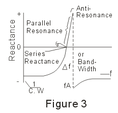
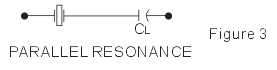
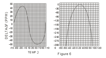
FREQ. Vs. TEMPERATURE
-40°C ~85°C , from low temp. 5°C step up to high temp
Glass Sealed Ceramic Surface Mount Crystal Package
MECHANICAL CHARACTERISTICS
VIBRATION
20G, 10~2000Hz sweep for 20 minutes, 1.52mm, 4 hours for each direction.
Ref. MIL-STD-883E Method 2007.2
MECHANICAL SHOCK
100G, 0.5mS, 3 times for each direction
Ref. MIL-STD-883E Method 2002.3
DROP TEST
75cm Height.3 times on 2mm stainless plate.
Ref.JIS C6701
SOLDERABILITY
95% Coverage by using 63/37 solder at 230±5°C solder pot immersion 3±0.5 seconds.
Ref.MIL-STD-883E Method 2003.7
RESISTANCE TO SOLDER HEAT
10 Seconds 5 seconds immersion into 260±5°C solder pot. Ramp rate is 1 to 4°C/sec; above 183°C is 90~120 seconds.
Ref. MIL-STD-202 Method 210, test condition J.
GROSS LEAK TEST
5kgf/cm Helium bombing for 2 hours, bubble test in 125±5°C FC # 40 for 60 Second or equivalent auto test method.
Ref. MIL-STD-883E Method 1014.10
FINE LEAK TEST
5kgf/cm Helium bombing for 2 hours, leak rate less than 1 10 exp (-8)atm.c.c./sec.
Ref.MIL-STD-883E Method 1014.10
DIMENSION CHECK
X, Y, Z, Three dimensional, according to specifications
Ref. MIL-STD-883E Method 2016
DPA (INTERIOR CHECK)
Visual and 50X Stereo-microscope.
Ref. MIL-STD-883E Method 2013.1
ENVIRONMENTAL CHARACTERISTICS
THERMAL SHOCK
-55°C~125°C for 100 cycles, dwell time: 30 minutes,
Transit time less than 10 minutes
Ref. MIL-STD-883E Method 1011.9
HIGH TEMPERATURE STORAGE
125±3°C 1000±12hours.
Ref. MIL-STD-883E Method 1055.4
LOW TEMPERATURE STORAGE
-55±3°C static 1000±12hours.
Ref. MIL-STD-833E Method 1013
HIGH TEMPERATURE AND HIGH HUMIDITY STORAGE
85°C, RH 95%, 1000±12hours.
Ref. MIL-STD-833E Method 1004.7
FREQ. Vs. TEMPERATURE
-40°C ~85°C , from low temp. 5°C step up to high temp
| 
-Ov.gif)